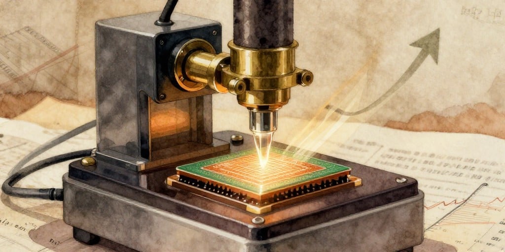
Teradyne Inc. Shares Surge Amid Minor Ownership Adjustment
On October 2 2026, Teradyne Inc. filed a Form 4 report with the U.S. Securities and Exchange Commission (SEC) detailing a transaction by Johnson Mercedes that involved the sale of a small block of the company’s common stock. The transaction was executed under a pre‑approved sales plan to comply with Rule 10b‑5‑1 of the Securities Exchange Act, and it was reported that Johnson Mercedes retained both a direct ownership stake and an indirect holding through a trust, with the company acting as trustee and sole beneficiary. The filing confirmed that the ownership change occurred on the first day of the reporting period (2026‑10‑01) and was submitted the following day.
The SEC filing, while limited in scope, included standard corporate information—Teradyne’s headquarters address in North Reading, Massachusetts, and its industry classification as an instrument manufacturer for the measurement and testing of electrical signals. No financial statements or performance metrics were disclosed, and the transaction did not represent a material change in the company’s capital structure.
Market coverage from German financial media reported that Teradyne’s share price performed strongly within broader U.S. equity indices. In the Nasdaq‑100, the company was identified as one of the best‑performing stocks for the day, recording a moderate percentage increase. In the S&P 500, Teradyne ranked among the top gainers, reflecting a comparable rise in its share value. These reports underscore the company’s continued visibility and positive momentum in the market, even in the absence of new earnings or guidance announcements.
Corporate Implications of the Transaction
The transaction constitutes a routine share‑sale event, with no material impact on the company’s governance or strategic direction. Johnson Mercedes’ continued direct and indirect holdings suggest ongoing confidence in Teradyne’s business model and its role as a critical supplier of precision testing equipment to semiconductor manufacturers. The retention of an indirect holding through a trust may provide a layer of diversification for Johnson Mercedes’ investment portfolio while ensuring a stable, long‑term relationship with Teradyne.
Semiconductor Technology Trends and Their Influence on Teradyne’s Business
Teradyne’s core product portfolio—automatic test equipment (ATE) and precision measurement instruments—serves as a foundational technology platform for semiconductor manufacturers as they advance to ever smaller process nodes. The following technical dynamics shape the industry and, by extension, the demand for Teradyne’s solutions:
| Trend | Node Progression | Yield Optimization | Technical Challenges |
|---|---|---|---|
| FinFET & Gate‑All‑Around (GAA) Scaling | 7 nm → 5 nm → 3 nm and beyond | Enhanced electrostatic control increases functional yield but raises defect sensitivity | Complex lithography, source‑drain engineering, and increased variability |
| EUV Lithography | 7 nm → 5 nm → 3 nm | Higher pattern fidelity improves yield, yet EUV introduces new defect modes | Cost of EUV tools, mask defectivity, and EUV‑specific process control |
| High‑K/Metal‑Gate (HKMG) Materials | 10 nm → 7 nm | Reduced short‑channel effects improve electrical performance | Interface quality, variability, and reliability across high‑K dielectrics |
| 3D Integration & TSV | 5 nm → 3 nm | Enables higher device density, improving functional yield per wafer | Through‑silicon via reliability, thermal management, and test accessibility |
| Advanced Packaging (Flip‑chip, Fan‑out‑on‑PAW) | 10 nm → 7 nm | Enhances performance and reduces parasitic capacitance | Package‑level yield, signal integrity, and test accessibility |
These advances necessitate more sophisticated test structures and protocols. Teradyne’s ATE systems must evolve to provide:
- Higher Test Throughput – To keep pace with the increased test cycles required by smaller nodes, ATE platforms need faster data acquisition and real‑time analytics.
- Advanced Test Modes – Including fault‑injection, power‑supply‑noise, and signal‑integrity testing, which become critical as device dimensions shrink.
- Integrated Design‑for‑Test (DfT) Support – As design complexity grows, incorporating DfT features such as Built‑In Self‑Test (BIST) and boundary‑scan becomes essential for yield optimization.
Manufacturing Processes, Yield, and Node Progression
Semiconductor manufacturing follows a tightly coupled cycle of design → fabrication → testing → packaging. Yield—defined as the ratio of functional chips to the total number of dies on a wafer—is influenced by:
- Defect density: Lower defect density yields higher functional yield. Advanced nodes demand sub‑nanometer defect control.
- Process variability: Variations in film thickness, doping concentration, and lithography focus affect device performance.
- Edge‑to‑edge consistency: Uniformity across the wafer mitigates yield loss due to peripheral defects.
As nodes shrink, the margin for yield loss shrinks dramatically. For example, moving from 7 nm to 5 nm can increase the critical dimension variation by 30 %, leading to a disproportionate decline in yield if not mitigated. Consequently, foundries invest heavily in statistical process control (SPC), in‑situ metrology, and machine learning–based yield management.
Capital Equipment Cycles and Foundry Capacity Utilization
Foundry capacity utilization is governed by a cyclical pattern of equipment procurement, ramp‑up, and depreciation. Capital equipment—particularly EUV lithography systems and advanced etch tools—requires multi‑year lead times and significant capital outlays:
- Equipment Cycle: Roughly 3–4 years from order to installation, with a 10‑year depreciation horizon.
- Capacity Utilization: Foundries often operate at 80–90 % capacity during peak demand for advanced nodes. However, utilization can drop during technology transitions or economic downturns.
- Capital Expenditure (CapEx): In 2026, total CapEx for the leading 3–5 nm nodes was projected to exceed $15 billion per year, with a large proportion dedicated to EUV tools and advanced lithography reticles.
Teradyne’s business is indirectly linked to these cycles. When foundries invest in new lithography tools, they must concurrently update their test infrastructure to handle the new design rules and process complexities. This creates a catalytic effect: capital spending on manufacturing equipment stimulates demand for advanced test equipment, which in turn encourages further CapEx in the foundry sector.
Interplay Between Chip Design Complexity and Manufacturing Capabilities
Modern chip design complexity has surged, driven by:
- Heterogeneous integration (CPU, GPU, AI accelerators, sensors, RF components).
- High‑performance logic and memory integration (e.g., 3D NAND, HBM).
- Advanced process technologies (e.g., 2 nm, 1.4 nm).
Design complexity imposes higher DfT demands. As logic density increases, traditional test approaches become impractical due to:
- Longer test times: More test patterns are required to cover the expanded logic space.
- Signal integrity challenges: Higher operating frequencies exacerbate timing errors.
- Power‑delivery constraints: Test power budgets must be managed carefully to avoid damage.
Manufacturing capabilities must therefore evolve in tandem. The introduction of design‑for‑manufacturing (DfM) guidelines and process‑aware design tools allows engineers to anticipate manufacturability issues early. Meanwhile, advanced simulation and modeling—including Monte Carlo and statistical process models—help predict yield outcomes before fabrication begins.
Technological Innovations Enabling Broader Advances
Semiconductor innovations act as an enabling foundation for a broad spectrum of technologies:
- Artificial Intelligence: Ultra‑low‑power, high‑density accelerators rely on advanced nodes to meet latency and energy budgets.
- Internet of Things (IoT): Miniaturized, low‑cost sensors and wireless modules necessitate scalable, high‑yield manufacturing.
- Automotive Electronics: Advanced driver‑assist systems (ADAS) require high‑reliability, high‑performance processors.
- 5G/6G Communication: RF front‑ends and baseband processors demand precise, high‑frequency devices fabricated on cutting‑edge nodes.
Each of these application domains drives further demand for precision test equipment capable of validating the increasingly sophisticated device architectures. Teradyne’s role as a provider of such equipment positions it to benefit from the continued push toward smaller process nodes and more complex system‑on‑chip (SoC) designs.
Market Perception and Investor Outlook
Despite the lack of new earnings or guidance in the SEC filing, Teradyne’s share price continued to perform well within the Nasdaq‑100 and S&P 500 indices. The minor ownership adjustment by Johnson Mercedes, while routine, signals confidence in the company’s strategic direction. Analysts may interpret the positive index performance as a reflection of:
- Stable demand for test equipment in a manufacturing landscape dominated by advanced nodes.
- Continued capital investment in both foundries and test equipment vendors.
- Robust supply chain resilience, as Teradyne’s equipment is essential for maintaining yield targets in high‑volume production.
In conclusion, Teradyne’s recent SEC filing illustrates a routine shareholder transaction amid a broader context of technological acceleration in semiconductor manufacturing. The company’s continued performance in major equity indices underscores the importance of precision test equipment as a critical enabler for advanced node production and the growing complexity of chip design. As foundries push further toward 2 nm and beyond, the interplay between manufacturing capabilities, capital equipment cycles, and design complexity will only intensify, cementing the role of vendors like Teradyne in the semiconductor ecosystem.