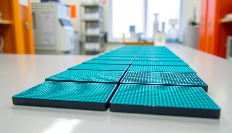
Shin‑Etsu Chemical Co. Ltd. Announces Breakthrough in 300‑mm GaN Substrate Technology
Shin‑Etsu Chemical Co. Ltd. (Japan) announced a technical milestone in its semiconductor materials division, reporting that its 300‑mm gallium nitride (GaN) growth substrate, branded QST™, achieved a record breakdown voltage of exceeding 650 V during testing of a 5‑µm high‑electron‑mobility transistor (HEMT) by the Belgian research institute IMEC.
Significance of the Achievement
- High‑Power Electronics
- The 650‑V breakdown voltage represents a substantial improvement over the current commercial baseline for GaN substrates, which typically range between 300–500 V.
- Higher breakdown voltage directly translates into greater power density and efficiency for devices such as RF amplifiers, power inverters, and electric‑vehicle (EV) traction converters.
- Market Positioning
- Shin‑Etsu’s QST™ platform has now demonstrated superior performance in a rigorous external benchmark, reinforcing its reputation as a leading supplier of advanced electronic materials.
- The achievement positions the company favorably against competitors such as CREE (now part of Cree, Inc.), Infineon Technologies, and ON Semiconductor, all of whom are actively developing high‑power GaN substrates for similar applications.
- Industry Implications
- The breakthrough aligns with the broader industry trend toward higher‑frequency, higher‑voltage power electronics driven by the rapid adoption of EVs, renewable energy systems, and 5G infrastructure.
- As power electronics shift toward GaN and silicon carbide (SiC) technologies, substrate performance becomes a critical differentiator.
Technical Context
GaN HEMT Structure
The 5‑µm HEMT test device leveraged the QST™ substrate’s inherent material quality and surface flatness to achieve the high breakdown voltage.
IMEC’s testing protocols, recognized for their rigor, provide strong validation of the substrate’s reliability under high‑power stress conditions.
Growth Process
Shin‑Etsu’s proprietary metal‑organic chemical vapor deposition (MOCVD) process for 300‑mm wafers enables precise control over defect density and layer uniformity—factors that critically influence breakdown behavior.
Economic and Competitive Landscape
| Segment | Current Drivers | Shin‑Etsu Position |
|---|---|---|
| Electric Vehicles | Demand for lightweight, high‑efficiency power converters | QST™ supports higher voltage modules, reducing system weight |
| Renewable Energy | Grid‑scale inverters require robust, high‑temperature components | Advanced substrate improves thermal stability |
| 5G Infrastructure | High‑frequency RF amplifiers need low‑loss, high‑power devices | Improved breakdown voltage expands operating envelope |
| Consumer Electronics | Miniaturization demands high‑power density components | Substrate quality enhances device longevity |
The semiconductor materials market is projected to grow at a compound annual growth rate (CAGR) of 7–9 % over the next five years, driven largely by the sectors highlighted above. Companies that can deliver substrates with superior electrical and thermal characteristics are likely to capture a larger share of high‑margin product lines.
Conclusion
Shin‑Etsu Chemical’s record‑setting breakdown voltage for its QST™ GaN substrate represents a meaningful technical advance with direct implications for the high‑power electronics market. By validating its materials through independent, high‑standard testing, Shin‑Etsu strengthens its competitive positioning and supports the broader industry shift toward next‑generation power conversion technologies.
