Corporate Insights into the Current Semiconductor Landscape
The recent downturn in European equity markets, driven in part by a muted performance in technology stocks, underscores the importance of understanding the underlying dynamics that shape the semiconductor industry. While investor sentiment may fluctuate, the sector’s evolution continues to be propelled by a confluence of technological milestones, manufacturing challenges, and capital‑intensive equipment cycles. This analysis examines the key drivers of node progression, yield optimization, and the technical hurdles that advanced chip production entails. It also considers how capital equipment life cycles, foundry capacity utilization, and the interplay between design complexity and fabrication capabilities influence the broader technology ecosystem.
Node Progression: From 5 nm to the 3 nm Frontier
Shrinking Feature Sizes: The transition from the 5 nm nodes that dominated the 2021‑2023 period to the 3 nm nodes being deployed in flagship processors marks a significant leap in transistor density. This reduction improves energy efficiency and performance per watt, which is critical for data‑center workloads and AI inference engines.
Technology‑Enabled Innovations: The 3 nm nodes incorporate high‑k metal‑gate (HKMG) stacks, gate‑length scaling, and more aggressive metal‑2/metal‑3 interconnects. These enable finer control of short‑channel effects and reduce parasitic capacitance, directly translating into higher clock speeds and lower power consumption.
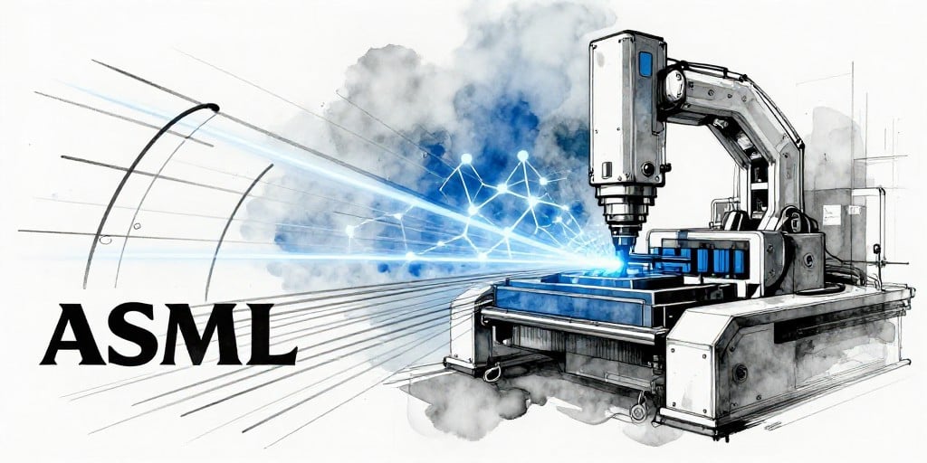
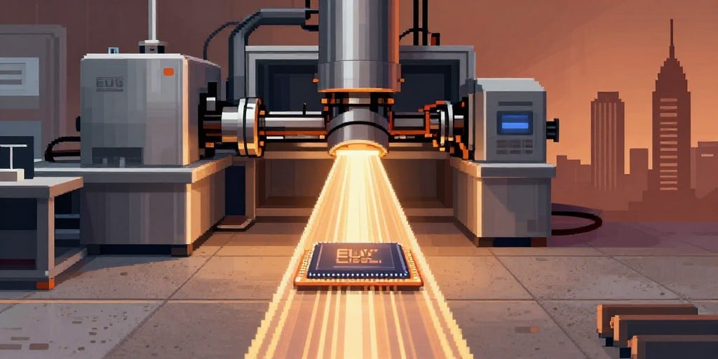
Manufacturing Complexity: As nodes shrink, lithographic demands intensify. Extreme ultraviolet (EUV) lithography at 13.5 nm wavelengths has become indispensable for patterning sub‑5 nm features. The reliance on EUV increases the need for cleanroom precision, resist technology, and alignment accuracy, all of which elevate yield risks.
Yield Optimization in the Advanced Node Era
Defect Density Management: With feature sizes approaching the nanometer scale, even a single defect can jeopardize a wafer. Foundries invest heavily in defect inspection technologies—such as high‑resolution optical and X‑ray inspection—to detect sub‑10 nm defects early in the process flow.
Statistical Process Control (SPC): Continuous monitoring of key process parameters (e.g., temperature, pressure, ion dose) allows foundries to apply SPC techniques to maintain process windows within tighter tolerances. This reduces process variance and enhances first‑pass yield.
Post‑Processing Enhancements: Techniques like wafer‑level packaging (WLP) and through‑silicon vias (TSVs) are employed to mitigate interconnect failures, improve thermal performance, and support 3D stacking. These steps, however, introduce additional yield challenges that must be addressed through meticulous design‑for‑manufacturing (DFM) guidelines.
Technical Challenges of Advanced Chip Production
Lithographic Precision: EUV exposure requires sub‑1 nm focus control. Any wavefront aberrations can cause critical dimension (CD) errors that propagate through the entire process flow. Advanced mask‑writing technologies, such as stepper lithography with high‑numerical‑aperture optics, are essential for maintaining pattern fidelity.
Material Innovation: The introduction of new dielectrics and metal stacks (e.g., high‑k/metal‑gate combinations) demands rigorous reliability testing. Issues such as dielectric breakdown and metal diffusion must be mitigated to preserve long‑term device performance.
Thermal Budget Management: Advanced nodes require precise thermal budgets to control dopant activation and interdiffusion. Over‑exposure can lead to feature swelling, while under‑exposure can cause incomplete activation, both detrimental to device yield.
Capital Equipment Cycles and Foundry Capacity Utilization
Equipment Lifecycle: High‑end lithography tools, such as the ASML 5.0 EUV steppers, have a typical useful life of 10–15 years. Their procurement involves multi‑year financing agreements, and the depreciation schedules impact the capital expenditure (CapEx) profile of foundries.
Capacity Utilization Trends: During periods of high demand—particularly for AI accelerators and high‑performance GPUs—foundries often run above 80 % utilization on 5 nm and 3 nm fabs. However, capacity constraints are exacerbated by the longer lead times for new EUV tool delivery, prompting foundries to diversify through mid‑node (7 nm, 10 nm) fabs to maintain revenue streams.
Strategic Partnerships: To mitigate capacity bottlenecks, many foundries form joint ventures or secure long‑term contracts with fabless designers. These agreements provide predictable demand, enabling foundries to justify the upfront CapEx required for next‑generation equipment.
Interplay Between Design Complexity and Manufacturing Capabilities
Design for Manufacturability (DFM): Modern chip designers increasingly rely on automated DFM checklists to ensure layout compliance with process‑specific constraints (e.g., minimum feature spacing, diffusion budgets). The tighter the design rules, the higher the potential yield, but this also limits creative freedom.
Heterogeneous Integration: The push toward system‑on‑chip (SoC) solutions, integrating CPUs, GPUs, AI accelerators, and specialized ASICs on a single wafer, demands sophisticated packaging techniques. 2.5D and 3D integration approaches introduce new interconnect and thermal management challenges that must be aligned with fab capabilities.
EDA Tool Evolution: As manufacturing processes advance, Electronic Design Automation (EDA) tools must incorporate more accurate process models, including variability and stochastic effects. This enables designers to predict yield outcomes more reliably, reducing risk for both designers and foundries.
Semiconductor Innovation as a Catalyst for Broader Technological Advances
Artificial Intelligence Acceleration: The enhanced transistor densities and lower power profiles of 3 nm nodes enable AI models to run at higher inference speeds with reduced energy consumption. This has direct implications for cloud service providers, autonomous systems, and edge computing devices.
Internet of Things (IoT) Expansion: Low‑power, high‑density silicon enables widespread deployment of IoT sensors, where cost and size constraints are paramount. Advanced process nodes allow for tighter integration of sensors, processors, and communication modules.
5G/6G Infrastructure: Telecom infrastructure demands chips with high throughput and low latency. The scaling benefits of advanced nodes support the massive bandwidth and low‑latency requirements of next‑generation wireless standards.
Conclusion
Despite short‑term market volatility, the semiconductor industry’s trajectory remains firmly anchored to technological progress. The relentless march toward smaller nodes, coupled with sophisticated yield optimization strategies and the strategic management of capital equipment cycles, continues to empower the next wave of digital transformation. Companies that successfully navigate the intricate balance between design ambition and manufacturing reality will be best positioned to capitalize on the opportunities presented by AI, IoT, and advanced communication networks.