
Corporate News – Market Reaction and Technical Context
Intel Corp. experienced a modest decline in its share price during the day, with trading activity reflecting a cautious market stance toward the semiconductor firm. The decline was small in magnitude but notable relative to the broader market movement, which included a mixed performance across major U.S. indices. While the broader technology sector showed resilience, with several chipmakers posting gains, Intel’s movement was a slight drop, signaling a tempered investor sentiment toward the company’s recent outlook.
Analysts noted that Intel’s position within the semiconductor landscape continues to be influenced by the rapid expansion of artificial‑intelligence applications, which have shifted some focus toward graphics‑processing units and other specialised accelerators. In this environment, Intel’s traditional central‑processing‑unit emphasis is being scrutinised as the market evaluates the relative value of its product lines in an AI‑driven economy. The company’s recent performance, therefore, reflects a broader reassessment of its role within the sector.
Market participants observed that while some chip names have benefited from AI‑related demand, Intel’s own share price has not mirrored that momentum to the same degree. This divergence has prompted discussions about the company’s strategic priorities and the pace of its product development cycle. Investors are monitoring the company’s guidance and any forthcoming updates on its technology roadmap, which could influence future pricing dynamics.
Node Progression and Yield Optimization
Intel’s recent performance must be viewed in the context of its ongoing node transition from 7 nm (tSMC‑based) to 5 nm and eventually to 3 nm processes. Each node transition brings significant yield challenges:
- Lithography and Etch Variability – As feature sizes shrink, the tolerance for line‑edge roughness and critical dimension variation increases. This has historically led to lower initial yields on early‑run wafers, especially in a design‑intensive environment such as AI inference.
- Complexity of 3D Integration – The move toward stacking memory and logic layers (e.g., through TSVs and micro‑bumps) introduces new thermal and stress management issues that can degrade yield unless carefully controlled.
- Process Integration of Heterogeneous Materials – Incorporating high‑κ dielectrics, new gate‑stack materials, and advanced interconnects requires additional process steps, each a potential source of defects.
Yield optimization strategies, such as aggressive defect‑inspection protocols and adaptive manufacturing tooling, are essential to maintain cost competitiveness. The modest share decline may reflect investors’ concern that yield ramp‑up timelines could be extended, affecting revenue projections.
Capital Equipment Cycles and Foundry Capacity Utilization
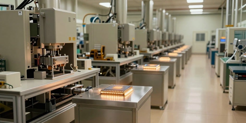
Capital equipment for advanced lithography (e.g., EUV scanners), deposition (ALD, CVD), and metrology (scatterometry, SEM) has a multi‑year procurement and deployment cycle. The semiconductor industry typically experiences a capital‑expenditure peak 2–3 years after a new node’s commercial launch, followed by a plateau as equipment reaches full utilization. Key points:
- Equipment Lead Time – EUV systems have an average lead time of 18–24 months. Any delay in delivery or commissioning can stall ramp‑up for the next node, pushing back product launches.
- Utilization Rates – Foundries often aim for >70 % utilization on advanced nodes to achieve cost recovery. However, low demand for niche CPU products can leave capacity underutilised, prompting foundries to shift production to higher‑volume logic or memory fabs.
- Secondary Market and Tool Sharing – The rise of “fab‑less” companies and IP‑based foundry services means that capital equipment may be shared across multiple product families, diluting the impact of a single firm’s production hiccup.
Intel’s current share dip may partially stem from expectations that its foundry operations (e.g., the IDM‑2 strategy) will face extended capacity utilization cycles, limiting the firm’s ability to quickly capitalize on AI‑driven demand.
Design Complexity vs. Manufacturing Capability
Modern AI workloads demand heterogeneous compute engines: large‑batch matrix multipliers, tensor cores, and low‑latency data‑movement units. This drives:
- Increased Design Rule Density – More transistors per unit area require tighter layout rules, which can increase design turnaround times and cost.
- Mixed‑Signal Integration – Combining analog front‑ends for AI accelerators with digital logic adds design complexity, particularly when targeting deep sub‑10 nm nodes.
- EDA Tool Evolution – Advanced physical‑design tools (e.g., for placement‑routing under high‑κ constraints) are essential, but their maturity can lag behind silicon technology, creating a bottleneck.
Intel’s CPU-centric roadmap must balance these demands against the manufacturing envelope of its 10 nm and 7 nm processes. Failure to align design complexity with process capabilities can lead to yield erosion, higher defect costs, and ultimately lower profitability—factors that are likely being weighed by the market.
Technological Innovations Enabling Broader Advances
Despite these challenges, semiconductor innovations continue to unlock new capabilities:
- FinFET and Gate‑All‑Around (GAA) Architectures – Provide superior electrostatic control, enabling higher transistor densities without significant leakage penalties.
- High‑Performance Interconnects – Copper‑on‑Silicon and carbon‑nanotube interconnects reduce RC delays, critical for high‑throughput AI inference pipelines.
- On‑Chip AI Accelerators – Integration of dedicated AI cores directly within CPUs or system‑on‑chip (SoC) designs reduces data movement overhead, lowering power consumption.
These technological strides reinforce the importance of a robust manufacturing pipeline. Intel’s ability to integrate such innovations into its product mix, while managing yield and capacity constraints, will likely dictate its future competitive positioning.
Market Implications and Forward Outlook
The nuanced decline in Intel’s share price suggests that investors are evaluating:
- Strategic Prioritisation – Whether Intel’s focus on CPU dominance remains viable in an AI‑first market dominated by GPUs and domain‑specific accelerators.
- Product Development Velocity – The timeline for delivering 3 nm or 2 nm products, which could close the performance gap with rivals.
- Capital Allocation – How Intel plans to fund capital‑intensive equipment purchases and whether it will seek partnerships or joint ventures to mitigate risk.
A clear, technology‑driven roadmap that demonstrates yield scalability, rapid capacity utilization, and a balanced portfolio of AI‑friendly products could restore investor confidence. Conversely, persistent uncertainty around node transition timelines or cost‑driven yield performance may continue to weigh on the stock.
This analysis integrates real‑world market dynamics with technical insights into semiconductor node progression, yield management, equipment cycles, and the interplay between design complexity and manufacturing capabilities. It highlights how Intel’s current performance reflects broader industry trends and the challenges inherent in advancing to the next generation of silicon.