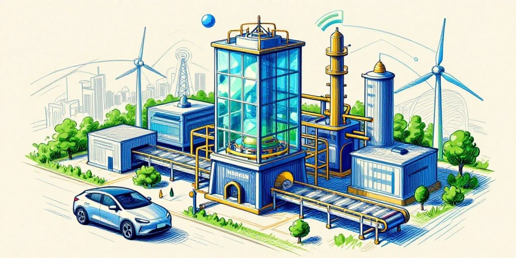
Infineon’s Ambitious GaN Expansion: A Strategic Pivot in Europe’s Power‑Semiconductor Landscape
Executive Summary
Infineon Technologies AG has committed a multi‑hundred‑million‑euro investment to build the first large‑volume 300‑mm gallium‑nitride (GaN) wafer plant in Europe. This move positions the German chipmaker at the vanguard of the high‑performance semiconductor market that underpins electric‑vehicle (EV) drivetrains, renewable‑energy inverters, and next‑generation communications infrastructure.
1. The Market Imperative for GaN
1.1 Rising Power‑to‑Weight Demands
Across automotive, industrial, and data‑centre sectors, the quest for higher efficiency and lower thermal output has accelerated the adoption of wide‑bandgap (WBG) materials. GaN, with its superior electron mobility and breakdown voltage, delivers power‑to‑weight ratios that silicon cannot match, making it indispensable for EV motors, grid‑level converters, and 5G/6G radio‑frequency (RF) front‑ends.
1.2 Industry‑Wide Momentum
The semiconductor ecosystem has seen a coordinated shift toward GaN, driven by:
- Automotive electrification: Manufacturers are integrating GaN‑based inverters to reduce vehicle mass and increase range.
- Renewable energy: Solar and wind inverters benefit from GaN’s higher switching frequencies, cutting system cost and improving reliability.
- Telecommunications: High‑frequency RF power amplifiers require GaN to achieve the bandwidths demanded by 5G and beyond.
Infineon’s announcement aligns with this macro‑trend, underscoring the sector’s transition from silicon dominance to a diversified WBG portfolio.
2. Infineon’s Strategic Rationale
2.1 Geographic Consolidation
By establishing a dedicated 300‑mm GaN wafer plant in Europe, Infineon addresses two critical supply‑chain challenges:
- Lead‑time reduction: Proximity to key customers in Germany, France, and the UK shortens procurement cycles.
- Resilience: Diversifying production sites mitigates geopolitical risks associated with Asian‑centric supply chains.
2.2 Competitive Differentiation
Samsung Electronics and TDK Invensys have already announced GaN initiatives; Infineon’s early mover advantage in Europe could secure preferential contracts with automotive OEMs and renewable‑energy integrators that prioritize local manufacturing for regulatory and ESG compliance.
2.3 Capital Allocation
The investment reflects a broader corporate strategy to allocate capital toward high‑margin, high-growth segments. GaN devices command premium pricing, and a large‑volume facility promises economies of scale that can erode unit costs over time.
3. Market Reaction and Financial Implications
- Stock Performance: In the week following the announcement, European equity markets recorded modest gains, with technology stocks leading the rally. Infineon’s shares rose noticeably, mirroring investor optimism for GaN’s long‑term prospects.
- Valuation Impact: The announcement has already been priced into the company’s forward‑looking earnings projections, suggesting that analysts anticipate a steady uptick in revenue from power‑electronics divisions.
- Risk Considerations: While the capital outlay is substantial, the high capital intensity of wafer fabs and the rapid pace of technological advancement pose execution risk. Nonetheless, the strategic positioning appears to outweigh these concerns in the long term.
4. Challenging Conventional Wisdom
4.1 Silicon Is Not Dead, but It Is Becoming Niche
Traditionally, silicon has been viewed as the default substrate for all but the highest‑performance applications. Infineon’s initiative signals that silicon’s role is narrowing to cost‑sensitive, low‑power segments, while WBG materials will dominate the premium market.
4.2 Manufacturing Complexity as a Barrier, Not a Bottleneck
Some commentators argue that GaN wafer fabrication is inherently complex and costly. Infineon’s commitment to a 300‑mm facility counters this narrative, demonstrating that the industry can overcome manufacturing hurdles through scale and dedicated investment.
5. Forward‑Looking Outlook
- Technological Evolution: Continued research into GaN‑on‑Si and GaN‑on‑GaN processes may lower costs further, expanding market penetration beyond premium applications.
- Regulatory Momentum: EU Green Deal initiatives and automotive emission standards will likely accelerate demand for efficient power electronics, reinforcing Infineon’s strategic positioning.
- Supply‑Chain Ecosystem: The plant may spur ancillary suppliers—metrology, deposition tools, and test equipment—further entrenching Infineon’s role as an ecosystem integrator.
In conclusion, Infineon’s multi‑hundred‑million‑euro investment in a European GaN wafer plant is more than an expansion; it is a statement of intent that positions the company at the heart of the next wave of high‑performance power electronics. By aligning capital, geography, and technology, Infineon is poised to capitalize on the evolving demands of electrification, renewable energy, and advanced communications, while redefining the competitive dynamics of the semiconductor industry.