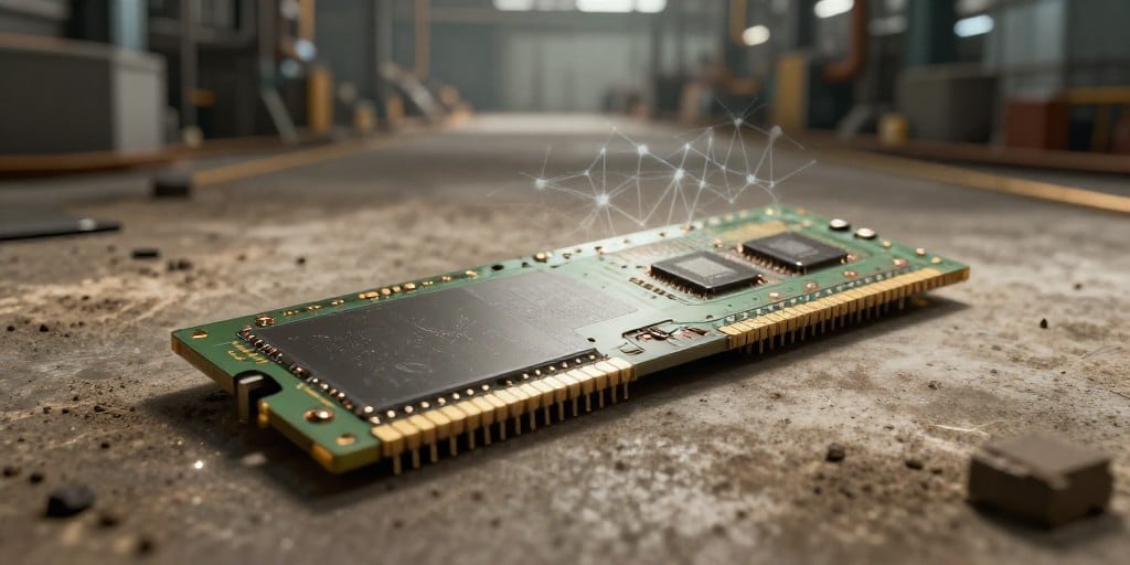
Corporate Update on Kioxia Holdings Corp. and Broader Semiconductor Dynamics
Kioxia Holdings Corp. has experienced a pronounced decline in its share price following a cautious earnings outlook that fell short of market expectations. The Japanese memory‑chip manufacturer’s guidance for the October‑December quarter projected operating profit of approximately ¥2 billion, slightly below the ¥2.35 billion consensus estimate. This discrepancy was sufficient to unsettle investors who had linked Kioxia’s valuation to the rapid expansion of artificial‑intelligence (AI) workloads that heavily rely on high‑density memory.
The sell‑off pushed the stock down by more than 15 % and left it considerably below the peak reached earlier in the year. The drop occurred amid a broader context of volatility in technology stocks across Asia, where gains in South Korea and China were offset by losses in Japan and Taiwan. Market participants expressed concerns that the rapid expansion observed in the AI sector may be cooling, a view that is reflected in the muted performance of other semiconductor names such as Tokyo Electron and Panasonic, which managed to post gains despite the wider sell‑off. In Tokyo, the Nikkei index finished the day slightly lower, while the broader Topix index slipped, illustrating the mixed mood in the market.
Currency markets showed limited movement, with the yen trading near its mid‑level against the dollar, and oil prices easing after diplomatic discussions that raised hopes of reduced supply disruptions. The overall sentiment in Asian equities remained cautious as investors weighed the implications of the AI‑driven rally against the backdrop of a slowing technology cycle and the potential need for a reassessment of valuations in the sector.
Technical Context: Semiconductor Trends and Manufacturing Challenges
Node Progression and Yield Optimization
The industry’s relentless push toward smaller process nodes—currently focused on sub‑10 nm nodes for logic and 3D‑stacked DRAM for memory—remains the cornerstone of performance and density gains. However, each reduction in feature size introduces a new set of lithographic and defect‑control challenges. For memory vendors like Kioxia, the transition from 3D‑XPoint‑derived 3D‑DRAM to 4 nm‑scale NAND requires:
- Enhanced EUV Lithography: Achieving high‑resolution patterning while maintaining acceptable defect rates demands continued investment in multi‑patterning techniques and source‑mask‑optimization strategies.
- Die‑to‑Die Uniformity: Yield is increasingly limited by variations in film thickness and etch depth across the wafer, necessitating advanced in‑line metrology and statistical process control.
- Defect Repair and Redundancy: The use of error‑correcting codes (ECC) and redundancy schemes must evolve to tolerate the higher defect densities associated with finer nodes.
Yield optimization has become a critical differentiator; even a 1 % improvement in die‑level yield can translate into a multi‑percentage point boost in revenue due to the high cost of advanced process equipment.
Manufacturing Processes and Technical Challenges
- Advanced Etch Chemistry: To maintain aspect ratios at sub‑10 nm, etch chemistries must achieve high selectivity and minimal damage to underlying layers. Innovations such as plasma‑enhanced chemical vapor deposition (PECVD) with nitrogen‑rich precursors are being explored to mitigate interface traps.
- Materials Integration: The adoption of high‑k/metal‑gate stacks and low‑k dielectrics in memory cells is essential for reducing parasitic capacitance, yet introduces issues of dielectric breakdown and thermal mismatch.
- Thermal Budget Management: As process steps become more temperature‑sensitive, careful sequencing of annealing steps is required to avoid dopant diffusion that would degrade channel performance.
Capital Equipment Cycles and Foundry Capacity Utilization
The semiconductor manufacturing ecosystem is heavily influenced by the cadence of capital equipment introductions. Key equipment vendors—such as ASML, Tokyo Electron, and Applied Materials—release new lithography, deposition, and inspection systems on multi‑year cycles. These cycles align closely with the industry’s node roadmap:
- EUV Lithography Adoption: The deployment of EUV tools has accelerated in the past five years, but the high cost (~$15 million per system) and the need for multiple units per foundry restrict rapid scaling.
- Automation and AI‑Driven Process Control: New generation of robotic assembly lines and AI‑enabled quality inspection systems promise to reduce cycle times and improve consistency, but require significant upfront investment.
Foundry capacity utilization has been strained by the surge in demand for AI accelerators and high‑performance computing workloads. Many fabs, especially those operating at advanced nodes, operate near full utilization, which can constrain the ability to absorb new orders from memory makers like Kioxia. This pressure is prompting strategic partnerships and co‑investment agreements to secure capacity for high‑margin products.
Interplay Between Design Complexity and Manufacturing Capabilities
Modern chip design increasingly leverages:
- Heterogeneous Integration: Combining logic, memory, and analog blocks on a single package (3D‑IC, TSV, silicon‑interposer) requires precise alignment and thermal management.
- Algorithmic Optimization: AI workloads demand specialized accelerators, which in turn push design teams to engineer ultra‑low‑latency memory interfaces.
- Security and Reliability Features: Incorporation of secure boot, encryption cores, and fault‑tolerant memory necessitates additional layers of silicon, affecting die size and yield.
Manufacturing capabilities must evolve in tandem. For example, the adoption of extreme‑high‑frequency (EHF) CMOS processes to support AI inference engines is contingent on the availability of fine‑pitch lithography and robust interconnect technologies. Simultaneously, memory vendors must design their stacks to accommodate these advanced logic layers without compromising endurance or data retention.
Semiconductor Innovations Driving Broader Technology Advances
- Higher Memory Density and Lower Power: 3D‑DRAM and resistive RAM (RRAM) innovations enable memory densities exceeding 1 Tb per wafer, supporting larger AI models and reducing power consumption in data centers.
- Near‑Edge Computing: Ultra‑low‑latency memory interfaces allow edge devices to perform inference locally, reducing dependence on cloud services and enhancing privacy.
- Advanced Packaging: Co‑process techniques such as through‑silicon via (TSV) and micro‑bump bonding improve signal integrity and thermal performance, facilitating integration of GPUs, CPUs, and memory on the same package.
- Process Node Scaling for AI: Sub‑7 nm logic nodes provide the transistor density required for high‑throughput matrix operations, essential for training deep neural networks.
These innovations are not isolated; they create a virtuous cycle where improvements in one area (e.g., memory technology) unlock performance gains in another (e.g., AI inference), which in turn fuels demand for even more advanced manufacturing capabilities.
Outlook for Kioxia and the Semiconductor Landscape
Kioxia’s recent earnings outlook reflects the broader caution in the memory sector, driven by a combination of overcapacity, volatile raw‑material costs, and the need for further process node reductions to stay competitive in AI workloads. While the immediate impact on its share price is significant, the company’s long‑term trajectory will hinge on its ability to:
- Secure Foundry Capacity: Align with foundries that can deliver advanced nodes (e.g., 4 nm or below) at competitive yields.
- Invest in Yield‑Enhancing Technologies: Adopt cutting‑edge lithography, defect‑repair, and process monitoring systems.
- Expand Product Portfolio: Diversify into emerging memory technologies such as 3D‑XPoint and RRAM to capture new market segments.
For the broader semiconductor ecosystem, the convergence of advanced manufacturing, sophisticated design paradigms, and capital equipment innovation will continue to dictate growth trajectories. Investors and industry stakeholders must monitor how effectively firms translate node progress into yield improvements and how rapidly they can scale production to meet the escalating demands of AI, autonomous systems, and high‑performance computing.