
Fujifilm Holdings Corp. Expands Semiconductor‑Materials Production
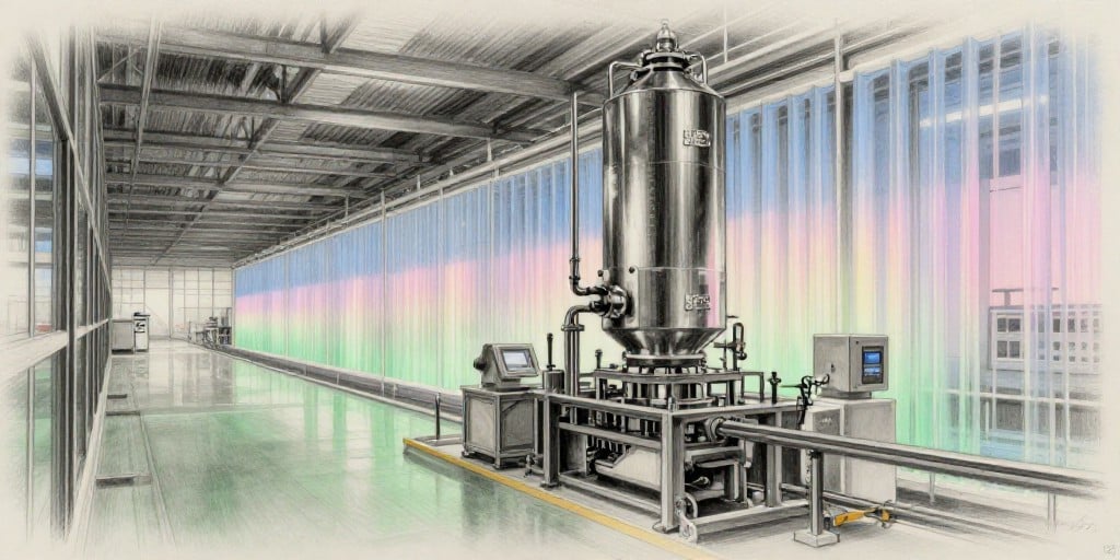
Fujifilm Holdings Corp. announced a substantial expansion of its semiconductor‑materials manufacturing capacity. The Tokyo‑based conglomerate will establish a new fabrication facility in Oita Prefecture, Japan, with the objective of tripling the output of post‑chemical‑mechanical polishing (CMP) cleaners. These cleaners are essential for the removal of microscopic particles and residues that remain on silicon wafers after the CMP process—a step that has become increasingly critical as global data‑centre growth, particularly in artificial intelligence (AI) workloads, demands higher precision in semiconductor fabrication.
Strategic Context
The investment—estimated at roughly ¥7 billion (≈ $44 million)—underscores Fujifilm’s deliberate pivot from its long‑standing camera and office‑equipment businesses toward the high‑growth semiconductor sector. Over the past year, revenue from the semiconductor‑materials segment has already increased by about 25 percent, reflecting both rising demand and the company’s expanding product portfolio. In addition to CMP cleaners, Fujifilm is developing complementary materials such as CMP slurries, photoresists, polyimides, and other lithography and packaging chemicals, positioning itself as a one‑stop supplier for advanced fabrication processes.
Market Dynamics
The semiconductor industry’s accelerated adoption of AI has amplified the need for ultra‑clean processing steps. Post‑CMP cleaning is a bottleneck in wafer fabrication; any contamination can compromise device yield and performance. Consequently, providers of CMP chemicals have experienced heightened demand, especially in regions with dense data‑centre infrastructure. By investing directly in production capacity, Fujifilm seeks to secure supply chain resilience and capture a larger share of this growing market.
Corporate Restructuring
Simultaneously, Fujifilm is exploring a spin‑off of its legacy business units, which continue to represent a substantial portion of overall revenue. A separate entity would allow for more agile investment decisions in the semiconductor‑materials domain, free from the capital‑intensive constraints of its traditional divisions. This strategic realignment aims to streamline operations and accelerate innovation in high‑margin growth areas.
Technological Innovation
The company has also begun deploying artificial‑intelligence‑driven tools to expedite chemical development. By leveraging AI algorithms, Fujifilm can identify optimal formulations for new materials within months rather than the years historically required. This capability not only shortens time‑to‑market but also reduces research and development costs, enhancing competitiveness against incumbents and emerging challengers.
Competitive Positioning
Fujifilm’s expansion positions it against established semiconductor‑materials suppliers such as ASML, 3M, and DuPont, as well as niche players that specialize in CMP chemicals. By combining scale, advanced R&D capabilities, and a diversified product line, Fujifilm aims to differentiate itself on both quality and innovation. The company’s focus on AI‑driven development further aligns its offering with the industry’s shift toward automation and data‑centric manufacturing processes.
Broader Economic Implications
The investment reflects a broader trend of traditional conglomerates reallocating resources toward high‑technology sectors that promise superior growth prospects. As data‑centre construction and AI adoption continue to rise, the semiconductor supply chain will experience sustained expansion. Companies that can secure critical materials—particularly those that influence wafer cleanliness and yield—will likely enjoy robust profitability. Fujifilm’s proactive stance aligns with this trajectory, potentially positioning the firm as a key partner in the next wave of semiconductor manufacturing.
This article provides a neutral, analytical overview of Fujifilm Holdings Corp.’s recent expansion into the semiconductor‑materials market, highlighting strategic, operational, and technological dimensions that may inform stakeholders across related industries.