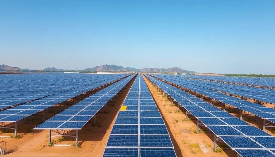
Corporate Analysis of First Solar Inc. in the Context of Semiconductor Innovation
Market Performance and Sector Dynamics
First Solar Inc., a U.S.-based manufacturer of thin‑film solar modules, has experienced a sustained range-bound movement in its stock price, a pattern that mirrors the volatility of the broader equity markets. Analysts attribute the company’s relative stability to its positioning within the expanding solar encapsulation segment—a niche that is expected to grow in tandem with heightened solar installation activity and advancements in photovoltaic panel technology. The firm’s performance remains intrinsically linked to the renewable‑energy sector’s resilience and the persistent demand for reliable photovoltaic components.
Semiconductor Technology Trends Shaping Photovoltaic Manufacturing
While the solar industry traditionally focuses on material science and module assembly, the underlying semiconductor processes that fabricate thin‑film layers are increasingly influencing manufacturing economics and product performance. Key trends include:
| Trend | Technical Impact | Implication for First Solar |
|---|---|---|
| Node Progression Beyond 28 nm | Adoption of 14 nm and 7 nm CMOS nodes for ancillary control ICs within module packaging. | Enables higher power‑to‑size ratios and reduced packaging costs. |
| 3D Integration & Through‑Silicon Vias (TSVs) | Integration of power electronics (e.g., bypass diodes, MPPT controllers) directly onto the module substrate. | Reduces interconnect losses and enhances module durability. |
| Advanced Lithography (EUV, DSA) | Higher resolution patterning for ultra‑thin active layers in CdTe or CIGS cells. | Improves carrier collection efficiency and yields. |
| Materials‑by‑Design Platforms | Use of high‑k dielectrics and novel alloyed semiconductors to tune bandgaps. | Allows perovskite‑cIGS tandem modules with >25 % efficiency. |
These innovations are not merely incremental; they represent a paradigm shift in how photovoltaic modules are engineered, directly affecting both cost structure and performance envelope.
Manufacturing Processes and Yield Optimization
Thin‑Film Deposition Techniques
- Chemical Vapor Deposition (CVD) and Molecular Beam Epitaxy (MBE) are being refined to deliver sub‑nanometer control over layer thicknesses.
- Plasma‑Enhanced Chemical Vapor Deposition (PECVD) offers lower temperature processing, critical for flexible substrates.
Yield optimization in such processes hinges on:
- Uniformity Control – Achieved through advanced in‑situ metrology (e.g., spectroscopic ellipsometry) to monitor film growth in real time.
- Defect Management – Implementation of defect‑dense patterning via EUV lithography reduces dislocation densities in III–V layers.
- Process Integration – Co‑optimization of deposition, annealing, and interfacial engineering steps reduces inter‑layer stress and enhances module longevity.
Capital Equipment Cycles
Semiconductor fabs operate on a capital‑intensive, multi‑year equipment cycle. First Solar’s integration of semiconductor‑grade deposition chambers and EUV lithography tools signals a commitment to staying on the cutting edge of node progression. However, these investments come with:
- High Up‑front CAPEX – Often exceeding $1 B per fab.
- Long Payback Periods – Dependent on module yield, pricing pressure, and demand growth.
- Equipment Utilization Constraints – Lower utilization rates can erode the cost advantage, especially during market downturns.
Balancing these factors requires a nuanced capital allocation strategy that aligns with the company’s projected production scaling and market expansion plans.
Foundry Capacity Utilization and Industry Dynamics
The semiconductor foundry sector has seen a gradual shift toward higher utilization rates as capacity constraints tighten. First Solar’s manufacturing footprint is influenced by:
- Foundry Partnerships – Collaborations with leading fabs (e.g., TSMC, Samsung) provide access to advanced nodes, albeit at premium pricing.
- Shared Equipment Pools – Utilization of shared EUV systems across multiple fabrication lines can lower average costs.
- Capacity Flexibility – Ability to reconfigure fabs for different cell chemistries (CdTe, CIGS, perovskite) allows rapid response to market signals.
The interplay between design complexity and manufacturing capabilities is increasingly critical. As module designs incorporate more sophisticated power‑management ICs and multi‑junction architectures, the fabrication ecosystem must match this complexity with advanced process controls and integration techniques.
Enabling Broader Technology Advances
Semiconductor innovations are not isolated to the manufacturing floor; they cascade into wider technology domains:
- Smart Grids – On‑module intelligence enables real‑time monitoring and predictive maintenance, reducing grid downtime.
- Energy Storage – High‑efficiency power electronics facilitate seamless integration with battery systems, accelerating renewable penetration.
- Artificial Intelligence – Edge computing modules powered by integrated ASICs can process sensor data directly on the solar panel, opening new service models.
By embedding semiconductor excellence into its product line, First Solar positions itself to drive not only incremental efficiency gains but also transformative shifts in how renewable energy is generated, managed, and consumed.
Conclusion
First Solar Inc.’s stock performance reflects broader sector dynamics, yet the company’s long‑term trajectory will be shaped by its capacity to integrate cutting‑edge semiconductor technologies into its manufacturing processes. Mastery of node progression, yield optimization, and capital‑equipment management will be pivotal in sustaining competitive advantage and capitalizing on the projected expansion of the solar encapsulation market.
