
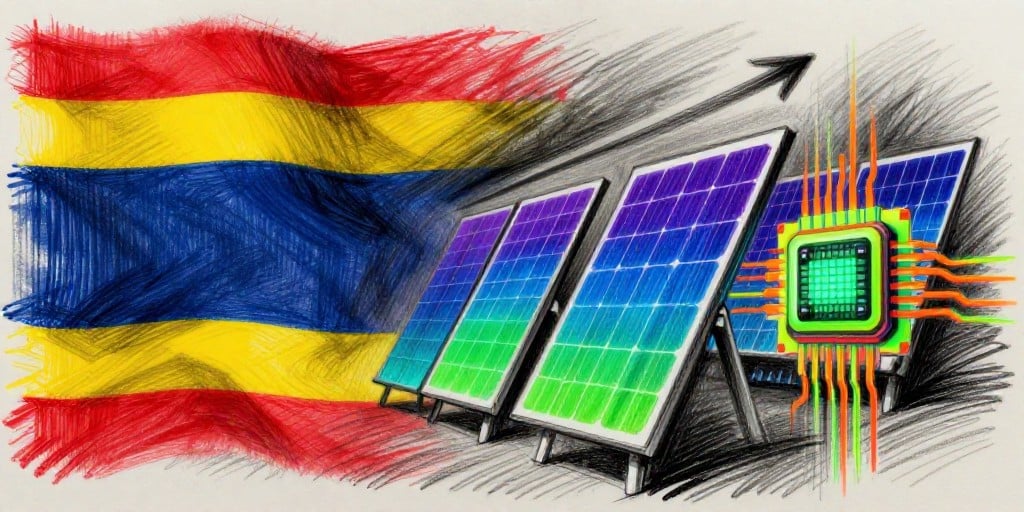
First Solar’s Entry into Thailand: A Catalyst for Technological and Capital Market Dynamics
First Solar Inc. has recently expanded its global footprint by launching a depositary receipt (DR) on the Stock Exchange of Thailand under the ticker FSLR03. The listing, which commenced trading on 16 July 2026, offers Thai investors exposure to the U.S. company’s thin‑film cadmium‑telluride (CdTe) solar panels, a product line that has long been a mainstay of First Solar’s portfolio. The DR’s structure— a direct listing with a conversion ratio aligned to the underlying Nasdaq price and adjusted for exchange and administrative costs—ensures that the Thai market gains a seamless conduit to First Solar’s growth prospects.
This move is part of a larger initiative by the Thai exchange to broaden its depositary receipt offerings across technology, energy, and semiconductor sectors. By incorporating a clean‑energy leader into this mix, the exchange signals a sustained appetite among Thai investors for companies that drive global sustainability and renewable energy deployment.
In addition to the market expansion, First Solar’s key customer, P.A. Resources Bhd, has reaffirmed its long‑standing supply agreement. The Malaysian aluminium extrusion company—whose profiles are integral to First Solar’s photovoltaic modules—has renewed a multi‑year contract that secures a steady supply of critical raw materials. The renewal is concurrent with P.A. Resources’ expansion plans, which aim to diversify its revenue beyond solar and to increase production capacity.
While the above developments are of immediate corporate significance, they also intersect with broader semiconductor technology trends and capital market dynamics. Below is an expert analysis of how these factors—node progression, yield optimization, manufacturing challenges, capital equipment cycles, and foundry capacity utilization—shape the industry’s trajectory.
1. Node Progression and Yield Optimization in Advanced Semiconductor Manufacturing
The semiconductor industry has historically progressed along a predictable trajectory of decreasing feature sizes, commonly referred to as node progression. This progression—from 7 nm to 5 nm, 3 nm, and now the nascent 2 nm nodes—has been driven by the need for higher transistor density, lower power consumption, and improved performance.
Yield optimization remains a critical metric as nodes shrink. With each successive node, the process window narrows, making fabrication more sensitive to variations in lithography, etching, and material properties. Yield loss is typically attributed to:
- Lithographic Defects: As feature sizes approach the wavelength of the exposure light, resolution limitations cause pattern distortions. Techniques such as extreme ultraviolet (EUV) lithography, double patterning, and directed self‑assembly (DSA) are employed to mitigate these effects.
- Etch Non‑Uniformity: Advanced transistors often contain high‑k/metal‑gate stacks that are highly susceptible to etch variations. Process control engineering (PCE) teams use real‑time monitoring and adaptive control to keep the etch rate within tight tolerances.
- Material Inhomogeneity: At sub‑3 nm nodes, interfacial roughness, dopant diffusion, and gate‑oxide thickness variations can cause significant device mismatch. New materials such as hafnium‑oxide or titanium‑oxide are being explored to provide better control over dielectric properties.
Yield optimization techniques, such as statistical design of experiments (DOE) and process‑by‑process modeling, are essential. These approaches allow fab managers to pinpoint the root cause of defects and to implement targeted corrective actions that reduce scrap rates and improve first‑pass yield.
2. Technical Challenges of Advanced Chip Production
As nodes shrink, several technical challenges arise that test the limits of current fabrication technology:
| Challenge | Description | Mitigation Strategies |
|---|---|---|
| Lithography Limits | The diffraction limit restricts resolution with conventional deep‑UV (DUV) sources. | EUV lithography, multi‑patterning, DSA. |
| Short‑Channel Effects | Reduced channel length increases leakage currents. | Use of high‑k dielectrics, metal‑gate stacks, and fin‑FET structures. |
| Thermal Budget Constraints | High‑temperature steps can cause dopant diffusion and layer intermixing. | Low‑thermal‑budget annealing, rapid thermal processing (RTP). |
| Metal Interconnect Reliability | Scaling interconnects increases resistance and electromigration risk. | Adoption of copper with barrier layers, use of low‑k dielectric spacers. |
| Contamination Sensitivity | Particles and chemical residues become more detrimental at smaller geometries. | Ultra‑cleanroom environments, advanced surface chemistry controls. |
Overcoming these challenges requires a synergistic approach that blends process innovation, advanced metrology, and rigorous statistical control. For instance, machine‑learning algorithms are increasingly being used to predict defect clusters and to optimize process recipes in real time.
3. Capital Equipment Cycles and Foundry Capacity Utilization
The semiconductor fab’s capital equipment cycle is tightly coupled to node progression. Transitioning to a new node demands:
- New Lithography Tools: EUV scanners can cost upwards of $1 billion each. The capital outlay is justified only if the node delivers a sufficient competitive edge and the fab’s capacity utilization remains high.
- Metrology and Inspection Systems: As dimensions shrink, measurement tools such as scatterometers, spectrometers, and electron‑beam tools must achieve higher precision, driving up costs.
- Process Control Infrastructure: Real‑time monitoring systems and data‑analytics platforms require significant investment.
Foundries often adopt a “build‑for‑capacity” model: they construct new fabs with the capacity to scale up to a target utilization rate (typically 80–90 %). The capital equipment cycle thus aligns with the foundry capacity utilization cycle. When utilization dips below optimal levels, foundries may defer capital expenditure, sell excess equipment, or repurpose lines for older nodes—a strategy that preserves cash flow and maintains revenue streams.
In the context of First Solar, while the company itself is not a foundry, its reliance on advanced semiconductor components—such as power management ICs, thin‑film sensor arrays, and high‑efficiency charge‑collection circuits—places it within the ecosystem that drives demand for cutting‑edge fabrication processes. As such, any shift in foundry capacity utilization or equipment cycles can indirectly affect the cost structure and supply chain resilience of solar module manufacturers.
4. Interplay Between Chip Design Complexity and Manufacturing Capabilities
Modern chip design increasingly incorporates heterogeneous integration and system‑on‑chip (SoC) architectures. These designs demand:
- Mixed‑Voltage Domains: Balancing performance and power consumption across multiple voltage rails.
- Fine‑Granularity Power Domains: Allowing selective power gating to reduce idle leakage.
- Complex Interconnect Topologies: Supporting high‑bandwidth data paths while minimizing crosstalk.
Manufacturing capabilities must evolve to accommodate these demands. For example, 3D stacking and through‑silicon vias (TSVs) enable vertical integration of logic, memory, and I/O layers, thereby reducing interconnect length and improving performance. However, TSVs introduce their own manufacturing challenges, such as void formation, stress management, and thermal dissipation.
The semiconductor industry’s response has been the adoption of design‑for‑manufacturability (DFM) guidelines and foundry‑design‑rules that codify the tolerances and constraints of specific nodes. These guidelines help designers navigate the trade‑off between performance goals and manufacturability, thereby ensuring that the final product can achieve the promised yield.
5. How Semiconductor Innovations Fuel Broader Technological Advances
Semiconductor breakthroughs are the backbone of many emerging technologies:
- Photovoltaic Systems: Power management ICs with ultra‑low quiescent current extend the lifetime of solar panels. Advanced photodetectors and temperature‑sensing circuits enable real‑time monitoring and adaptive shading control.
- Energy Storage: High‑density, high‑cycle life batteries rely on integrated battery management systems that monitor cell temperature, state‑of‑charge, and health—all of which are enabled by advanced semiconductors.
- Internet of Things (IoT): Low‑power microcontrollers and radio transceivers, powered by efficient CMOS processes, enable massive sensor deployments in smart cities and industrial automation.
- Artificial Intelligence (AI): Edge AI chips that combine deep‑learning accelerators with power‑efficient memory subsystems reduce latency and bandwidth consumption in autonomous vehicles and drones.
The continuous improvement in node progression, yield optimization, and manufacturing robustness directly translates to higher performance, lower cost, and greater reliability of these technologies. Consequently, the broader tech ecosystem benefits from faster deployment cycles, more ambitious product roadmaps, and reduced barriers to entry for startups and innovators alike.
Conclusion
First Solar’s Thai DR listing not only broadens its investor base but also underscores the interconnectedness of the global semiconductor and renewable energy sectors. The company’s reliance on advanced semiconductor technologies—both in its solar modules and ancillary electronics—places it at the intersection of cutting‑edge manufacturing processes, capital equipment cycles, and design‑manufacturability dynamics. As the semiconductor industry continues to push the boundaries of node progression and yield optimization, the ripple effects will be felt across all technology domains, from clean energy to AI and beyond.