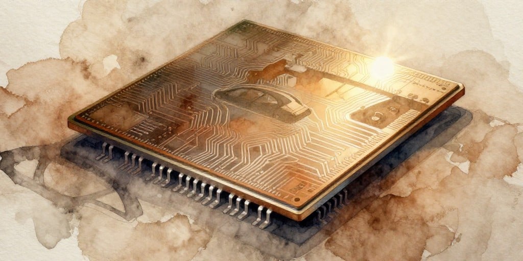
European Semiconductor Landscape Amidst AI‑Driven Market Dynamics
European equities recorded a muted performance on Wednesday, following a sharp downturn the prior day that stemmed from concerns over the speed of artificial‑intelligence (AI) capital deployment. While the broader index absorbed some of the earlier decline, the Dutch chip‑equipment conglomerate ASML Holding NV still managed a modest rise in its shares, underscoring sustained investor appetite for semiconductor innovation in a climate of falling commodity prices and a strengthening U.S. dollar.
The sectoral lift came in the context of a broader, cautiously optimistic market sentiment. The Stoxx‑600 and Euro‑Stoxx‑50 gained marginally, whereas the DAX slipped slightly. In London, the FTSE 100 edged down, pressured mainly by a fall in mining and energy stocks. The Swiss market remained largely unchanged, and German and French indices moved only marginally. Investors continue to monitor the forthcoming Anthropic initial public offering—a potential bellwether for AI‑driven growth—while awaiting clearer signals from central‑bank policy and inflationary trends.
Node Progression and Yield Optimization in Advanced Process Nodes
The relentless march from the 7 nm node to the 5 nm and now the nascent 3 nm and 2.5 nm regimes illustrates the semiconductor industry’s commitment to scaling while maintaining yield. Transitioning to sub‑7 nm nodes involves:
- Extreme Ultraviolet (EUV) Lithography – EUV has become the linchpin for patterning sub‑20 nm features. However, its high cost and limited exposure tools (ASML’s NXE‑3100) constrain foundry throughput and raise capital outlays.
- High‑k Metal‑Gate (HKMG) Technology – HKMG stacks reduce short‑channel effects but introduce variability in effective channel length and threshold voltage, necessitating sophisticated statistical process control (SPC) and design‑for‑manufacturability (DFM) strategies.
- Multi‑Patterning and Immersion Lithography – These techniques, while enabling finer pitches, add process steps that inflate defect density and complicate mask alignment, thereby influencing yield trajectories.
Yield optimization at these nodes is no longer a function of defect reduction alone; it also hinges on statistical design of experiments (DOE) and machine‑learning‑driven predictive models that anticipate defect clusters and process variations before they manifest on the wafer.
Advanced Manufacturing Processes and Technical Challenges
The leap to 3 nm and beyond introduces a host of technical obstacles:
- Pattern Transfer Fidelity – As critical dimensions shrink below 5 nm, even sub‑nanometer deviations in line‑edge roughness can precipitate catastrophic device failures.
- Material Reliability – New high‑k dielectrics such as La₂O₃ and TiN gate stacks demand improved deposition uniformity and thermal stability to avoid trap‑mediated leakage.
- Thermal Budget Constraints – Back‑end processes such as Cu redistribution layers must be engineered to withstand aggressive annealing cycles without compromising interconnect integrity.
These challenges compel foundries to adopt adaptive process control (APC) frameworks that leverage real‑time sensor data, coupled with predictive analytics to adjust lithography doses or etch chemistries on the fly.
Capital Equipment Cycles and Foundry Capacity Utilization
The semiconductor equipment supply chain operates on a multi‑year cycle that is tightly coupled to industry demand. Key observations:
- Capital Expenditure (CapEx) Peaks – The recent uptick in demand for EUV and 3D‑DRAM equipment has pushed ASML, Applied Materials, and Lam Research to expand their order books. Yet, the equipment lead time—often 18–24 months—means that capacity utilization peaks only after a lag.
- Capacity Utilization Trends – In 2024, European fabs such as ASML‑supported Samsung and GlobalFoundries reported utilization rates hovering around 75–80 % for the 5 nm node, with projected increases as 3 nm roll‑outs begin.
- Inventory Dynamics – The period of heightened demand has also strained raw‑material supplies (e.g., high‑purity silicon wafers, rare gases), prompting manufacturers to hold larger safety stocks, which in turn compresses the effective capacity available for new production lines.
Interplay Between Chip Design Complexity and Manufacturing Capabilities
The design‑manufacturing feedback loop has become more intricate than ever. Modern SoCs, particularly those targeting AI inference and training, incorporate:
- Large‑scale TPUs and ASICs that require heterogeneous integration (e.g., 3D‑stacked memory, silicon‑interposer links).
- Advanced packaging technologies like TSV and In‑FOG that impose stringent alignment tolerances and thermal constraints.
Manufacturing capabilities must, therefore, evolve in tandem. The adoption of chip‑on‑glass (COG) and chip‑on‑chip (COC) packaging, for instance, necessitates new etch chemistries and alignment systems that are not yet standard in conventional fabs.
Design teams now increasingly employ design‑for‑manufacturing (DFM) checks at early stages, using simulation tools that predict lithographic hotspots, doping profiles, and thermal budgets. These tools are fed back into process development, creating a virtuous cycle that improves both yield and time‑to‑market.
Semiconductor Innovations Driving Broader Technological Advances
Semiconductor breakthroughs ripple across multiple domains:
- Artificial Intelligence – High‑density, low‑latency accelerators benefit from smaller, power‑efficient transistors that reduce energy per inference operation.
- Internet of Things (IoT) – Ultra‑low‑power devices leverage advanced FinFET architectures and gate‑all‑around (GAA) transistors to maintain performance while extending battery life.
- Quantum Computing Interface – Classical control electronics for quantum processors rely on cryogenic‑compatible chips, requiring novel material stacks and packaging solutions that are being developed in parallel with standard CMOS nodes.
In each case, the scalability and reliability afforded by cutting‑edge semiconductor technology underpin the broader ecosystem’s evolution.
Outlook
The European semiconductor sector remains in a state of cautious optimism. While AI investment continues to galvanize interest, the capital intensity of next‑generation fabs and the technical complexity of emerging nodes impose a tempered pace on growth. Investors will likely focus on companies that demonstrate strong yield management, capability to scale capital equipment efficiently, and a robust DFM pipeline that aligns design complexity with manufacturing realities. As the industry progresses, the symbiosis between technological innovation and manufacturing prowess will dictate the pace at which new chips can be brought to market—and ultimately, how quickly the benefits of AI, IoT, and emerging technologies are realized worldwide.