
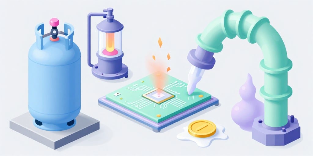
Entegris Inc. Announces Quarterly Dividend and Provides Insight into the Semiconductor Supply Chain
Entegris Inc. (NASDAQ: ENGR) filed a current report on July 15 2026, disclosing that its board of directors has declared a quarterly cash dividend of $0.10 per share. The dividend will be paid on August 19 2026 to shareholders of record as of the close of business on July 29 2026. The announcement, incorporated into the filing via a news release attached as Exhibit 99.1, is the sole material event reported for the quarter.
Entegris: A Critical Node in the Advanced Materials Ecosystem
Entegris positions itself as a supplier of advanced materials and process solutions that underpin the semiconductor and high‑technology sectors. Its operations span a global footprint—U.S., Canada, China, Germany, Israel, Japan, Malaysia, Singapore, South Korea, and Taiwan—supporting the full life‑cycle of chip manufacturing from wafer fabrication to final testing. ISO 9001 certification and a workforce of roughly 7,700 employees attest to the company’s commitment to quality and operational excellence.
Although the filing contains no new financial statements or performance data beyond the dividend declaration, the company’s forward‑looking statements highlight expectations regarding future dividend payments and other business developments, accompanied by a standard disclaimer about uncertainties.
Semiconductor Technology Trends and Their Impact on Entegris’ Business
Node Progression and the Drive Toward Smaller Features
The industry’s relentless march toward 7 nm, 5 nm, and eventually 3 nm nodes is accelerating demand for materials that can withstand higher temperatures, lower defect densities, and increasingly stringent process controls. Entegris’ portfolio—including specialty gases, high‑purity solvents, and advanced filtration systems—directly supports these nodes by ensuring ultra‑clean environments critical for lithography and chemical‑mechanical planarization (CMP). As nodes shrink, the acceptable contamination threshold tightens from parts‑per‑trillion (ppt) at 7 nm to sub‑ppt levels at 3 nm, amplifying the value of Entegris’ clean‑room solutions.
Yield Optimization and Defect Control
Yield optimization remains a top priority for foundries and integrated device manufacturers (IDMs). The cost of a single defect can exceed $10 000 at advanced nodes. Entegris’ process solutions—ranging from wafer‑level chemical vapor deposition (CVD) precursors to gas‑phase purification systems—reduce defect density by eliminating particulate and chemical impurities that could lead to yield‑degrading failures. Moreover, Entegris’ real‑time monitoring tools enable predictive maintenance, reducing downtime and improving overall yield.
Technical Challenges in Advanced Chip Production
High‑Temperature Processing Advanced nodes require temperatures above 1,200 °C for high‑k dielectrics and metal‑gate formation. Materials used in furnaces and gas lines must resist corrosion and outgassing. Entegris’ specialty alloys and coatings provide the necessary chemical stability and thermal conductivity.
Low‑Defect Lithography Immersion and extreme ultraviolet (EUV) lithography demand solvents and gases with extremely low total organic carbon (TOC) and water content. Entegris’ ultra‑pure gas delivery systems ensure that exposure tools receive flawless feedstock, thereby maintaining critical dimension control.
Material Compatibility with 2‑D and 3‑D Architectures Heterogeneous integration, such as silicon‑on‑insulator (SOI) and 3‑D stacked dies, introduces new interface challenges. Entegris’ expertise in deposition and etching chemistries facilitates the creation of high‑quality dielectric layers essential for these architectures.
Capital Equipment Cycles and Foundry Capacity Utilization
Equipment Modernization and the 10‑Year Capital Cycle
Semiconductor fabs operate on a 10‑year capital equipment cycle: from acquisition of lithography tools and deposition equipment to their eventual retirement. This cycle dictates the pace at which new nodes become commercially viable. Entegris’ services are synchronized with this cadence, offering pre‑manufacturing validation for new equipment and post‑manufacturing maintenance to extend tool life. The company’s global service network ensures rapid response times—critical when a tool failure can halt a wafer line for days.
Capacity Utilization Metrics
Recent industry data shows that foundry utilization rates hover around 85–90 % for mature nodes (10 nm and above), while advanced nodes (5 nm and below) exhibit 70–80 % utilization due to higher capital intensity and longer ramp‑up periods. Entegris benefits from this trend by supplying high‑volume consumables—such as specialty gases and filtration cartridges—whose sales are closely tied to foundry throughput. As foundries expand capacity for next‑generation nodes, Entegris’ demand for advanced material solutions will correspondingly grow.
Interplay Between Design Complexity and Manufacturing Capabilities
Design for Manufacturability (DFM)
Chip designers increasingly collaborate with foundries to incorporate DFM constraints, such as pitch limits, patterning rules, and defect tolerance. Entegris’ role is to translate these constraints into material specifications, ensuring that every layer of the chip—from active devices to interconnects—has the requisite purity and chemical stability. This partnership accelerates time‑to‑market by reducing costly re‑design iterations.
Scaling and the Emergence of New Architectures
The shift toward heterogeneous integration, chiplet architectures, and high‑bandwidth memory (HBM) imposes new demands on packaging materials, interconnects, and thermal management solutions. Entegris supplies advanced adhesive and sealant chemistries that support these architectures, enabling designers to pack more functionality into smaller footprints without compromising reliability.
How Semiconductor Innovations Enable Broader Technological Advances
Artificial Intelligence and Machine Learning The exponential growth in AI workloads requires high‑performance, low‑power GPUs and accelerators. Entegris’ supply of low‑residue deposition chemicals and high‑purity gases ensures that these devices maintain the stringent defect thresholds needed for consistent training and inference.
Internet of Things (IoT) and 5G/6G IoT devices demand chips that are both power‑efficient and cost‑effective. Entegris’ process solutions for silicon‑on‑insulator (SOI) wafers and high‑k dielectrics enable the production of RF front‑ends with superior linearity and reduced power consumption, essential for next‑generation wireless networks.
Quantum Computing Quantum processors rely on ultra‑clean environments to preserve qubit coherence. Entegris’ cryogenic‑compatible gases and low‑outgassing materials support the fabrication of superconducting circuits and topological qubits, facilitating breakthroughs in quantum technology.
Automotive Electronics and Autonomous Systems Safety‑critical automotive chips must achieve high reliability under extreme temperatures. Entegris’ high‑temperature alloys and specialized thermal management solutions help manufacturers deliver chips that meet ISO 26262 and other automotive safety standards.
Conclusion
Entegris Inc.’s recent dividend declaration underscores the company’s confidence in its strategic positioning within the semiconductor supply chain. As the industry accelerates toward ever-smaller nodes and more complex architectures, the demand for advanced materials and process solutions will intensify. Entegris’ global footprint, ISO‑certified operations, and deep expertise in clean‑room technologies place it at the nexus of technology innovation and manufacturing excellence, enabling the next wave of semiconductor‑driven advancements across multiple high‑technology sectors.